Optoelectronic Materials & 2D Systems
Prof. Steven Pei, Project Leader
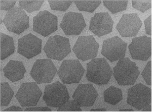
The optoelectronics Group has been concentrating its efforts in addressing the fundamental limitations of the carbon nanotube (CNT) and related materials for electronics device applications. Building on top of our pioneering work on the CVD growth of graphene on and its transfer off the metal substrate surface, which was recognized by Konstantin Novoselov in his Nobel Prize acceptance speech in 2010, the group also invented the seeded growth of single crystal graphene arrays at predetermined locations, which overcomes the degradation effects of the polycrystalline graphene grown by CVD and was featured on the cover of Nature Materials and also by Advanced Materials in 2011.
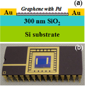
The group continues its investigation of the fundamental sciences of graphene and related 2D materials and devices. In particular, in collaboration with the Sandia National Laboratories, the team confirmed the growth-from-beneath mechanism of CVD bilayer graphene, which is completely against the commonly believe wedding cake growth model. The paper was selected by the editors of New Journal of Physics for inclusion in its exclusive ‘Highlights of 2012’ collection. The group also demonstrated the first field effect transistor fabricated on single crystal MoS2 and achieved record mobility and on-off ratio in 2013. Most recently, the group in collaboration with the Oxide Group also successfully fabricated single crystal WS2 grains. The emerging of a new class of 2D materials and heterostructures paves the way of the new generation of optoelectronic devices and sensors.
On the commercialization and international collaboration fronts, the group has established a number of collaboration with industry and foreign universities in Taiwan, China and Kazakhstan. The most noticeable one is the exchange and research collaboration agreement with the National Tsing Hua University in Taiwan. This collaborative program is supported by a $300,000 gift from the industry. Dr. Steven Pei has been appointed as an adjoin professor at the National Tsing Hua University , who is now supervising a graduate student at the National Tsing Hua University. Dr. Wei Wu was also appointed a visiting research assistant professor and spent a month conducting research in Taiwan in 2013. Another collaborative project involves Industrial Technology Research Institute (Hsinchu, Taiwan) and CAM members, Molex Inc. (Austin, TX) and The NSF Center for Electromagnetic Compatibility, to develop graphene coatings.
Other noticeable accomplishment is success of two spin-off companies from the group including the IPO of Applied Optoelectronics Inc. on NASDAQ (September 2013) manufacturing semiconductor optical interconnects for video and data systems, and the listing on the Chinese stock exchange of 2D Carbon (October 2015) which is manufacturing graphene touch screen for cell phones.
Publications
S. R. Xing, W. Wu, Y. A. Wang, J. M. Bao, and S. S. Pei, “Kinetic study of graphene growth: Temperature perspective on growth rate and film thickness by chemical vapor deposition,” Chemical Physics Letters, vol. 580, pp. 62-66, (2013).
N. Xie, H. Q. Gong, Z. Zhou, X. D. Guo, S. C. Yan, Q. Sun, S. R. Xing, W. Wu, S. S. Pei, J. M. Bao, X. Y. Shan, Y. Guo, and X. H. Lu, “Visualization of a Maze-Like Reconstruction of Graphene on a Copper Surface at the Atomic Scale,” Chinese Physics Letters, vol. 30, (2013).
W. Wu, D. De, S. C. Chang, Y. N. Wang, H. B. Peng, J. M. Bao, and S. S. Pei, “High mobility and high on/off ratio field-effect transistors based on chemical vapor deposited single-crystal MoS2 grains,” Applied Physics Letters, vol. 102, ( 2013).
Y. N. Wang, Z. H. Su, W. Wu, S. Nie, N. Xie, H. Q. Gong, Y. Guo, J. H. Lee, S. R. Xing, X. X. Lu, H. Y. Wang, X. H. Lu, K. McCarty, S. S. Pei, F. Robles-Hernandez, V. G. Hadjiev, and J. M. Bao, “Resonance Raman spectroscopy of G-line and folded phonons in twisted bilayer graphene with large rotation angles,” Applied Physics Letters, vol. 103, (2013).
J. M. Bao, S. R. Xing, Y. N. Wang, W. Wu, F. Robles-Hernandez, and S. S. Pei, “Fabrication of large-area twisted bilayer graphene for high-speed ultra-sensitive tunable photodetectors,” Micro- and Nanotechnology Sensors, Systems, and Applications V, vol. 8725 (2013).
W. Wu, Q. K. Yu, P. Peng, Z. Liu, J. Bao, S. S. Pei, and N. V. Lavrik, “Control of thickness uniformity and grain size in graphene films for transparent conductive electrodes,” Nanotechnology, vol. 23, (2012).
S. Nie, W. Wu, S. R. Xing, Q. K. Yu, J. M. Bao, S. S. Pei, and K. F. McCarty, “Growth from below: bilayer graphene on copper by chemical vapor deposition,” New Journal of Physics, vol. 14, Sep 17 (2012).