Photovoltaics & Nanostructures
Prof. Alex Freundlich, Project Leader
Photovoltaic and Nanostructures are addressed in an interdisciplinary approach to R&D problems in photovoltaic materials and devices. The project investigates a wide range of fundamental and applied materials problems to improve cell efficiency, increase power/weight ratios, and decrease the cost of high efficiency solar cells. Under development are sophisticated new III-V quantum-scale semiconductor materials and solar designs with projected efficiencies in excess of 50%, and new photovoltaic energy concepts that will enhance planetary and deep space exploration. The project is also the UH home to the recently established NSF/DOE Engineering Research Center (ERC) on “Quantum Energy Sustainable Solar Technologies”. The project is also instrumental in various educational and community outreach activities in solar Energy and has initiated related NSF supported REU and RET programs at UH.
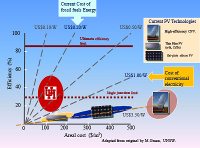
Ultra-efficient dilute nitrides MQW tandem designs In collaboration with its industry members, through the optimization of 1eV dilute nitride quantum well materials and design of multijunction solar cell the project demonstrated the possibility of synthesis of high quality dilute nitride heterostructures and a novel multijunction tandem design enabling higher practical efficiencies (~40% under 1 sun and 50% under 100 suns) well beyond the current State of the art for space (33%) and terrestrial concentrator (~42%) photovoltaics.
Single crystalline III-V semiconductor photovoltaics on flexible substrates Under the sponsorship of DOE-EERE “high impact photovoltaic manufacturing initiative”, the project focused on bridging the gap between unparalleled efficiencies demonstrated by eptaxial III-V semiconductor photovoltaic devices fabricated on expensive single crystalline substrate and low cost and somewhat inefficient thin film manufactured on inexpensive flexible metal templates. Building on the project’s pedigree in the heteropeitaxy of III-V semiconductors/development of defect tolerant devices and UH expertise in the development of highly textured crystalline template on flexible metals (for superconducting flat wires) the team was able to demonstrate the possibility of the realization of single crystalline GaAs epitaxial thin films on inexpensive flexible template. Also a new device was identified that when combined with the above mentioned innovation would support practical production efficiencies in excess of 13%, a nearly a two-fold improvement over the current a-Si based flexible module efficiencies (~6-7%) providing thus a clear pathway toward the deployment of low cost high efficiency flat panel modules.
Advances in the development of III-V nanostructures and in-situ diagnosis techniques The project continued its investigations for the development of highly ordered arrays of vertical III-V semiconductor nanorods, nanocones for improving light trapping and carrier transport in solar cells. The approach combined metal eutectic mediated VLS epi growths with established rapid and scalable techniques ( spin coating based nano-sphere lithography and holographic patterning). The investigation while directly supporting the needs in enhancing light absorption and minimizing reflective losses for off-normal incidence sunlight led the observation of nanowires with self-formation of embedded periodic zinc-blende/hexagonal crystal superlattices, a serendipity that could potentially have a major impact toward overcoming light absorption barriers in indirect bandgap semiconductor based devices . The team was also able to develop a new metrology technique based on reflection high energy electron diffraction (a common diagnosis tool on most vacuum based epi-techniques) and demonstrate the ability to extract real time the shape and size of epitaxial quantum dots with host of major applications for manufacturing of advanced photovoltaics and other emerging quantum-dot based devices.